These are pictures of a really magnificent photo detector I have.
They did a super job of RF design.
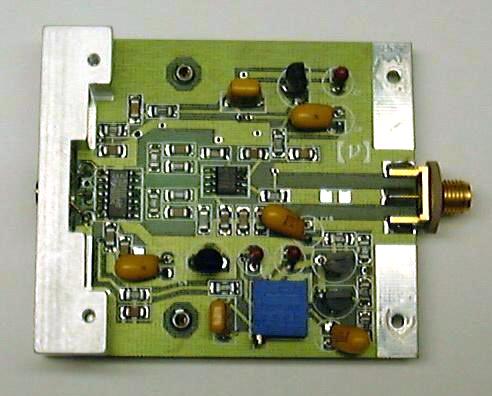
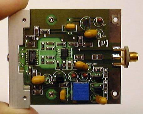
The circuitboard. At the left end is the detector, and at the right is the
output connector. Just look at how that connector is attached to the
board. You can also see the + and -15 Vdc connections. They are circular connectors
inside an octagonal area at the top and bottom of the board. Plenty of groundplane
on this circuit.
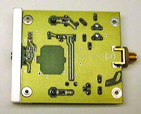
The back side of the board. Almost nothing but groundplane here. Look at the area
that was masked out. This must be some touchy low-level analog stuff that they
didn't want to have any stray capacitance to ground. Notice the diodes in series with the +/- power connections. This will keep you from trashing your
sensor if you connect the power supply backwards. I always appreciate it when manufacturers help me when I make a mistake.
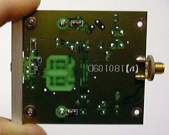
Backlit view of the back of the board.
Backlit view of the front of the board.
The power supply connections. They didn't want any of the RF signals getting
back out the power supply connections so they decoupled the power supply
leads on the outside of an aluminum plate to keep the RF inside where it belongs.
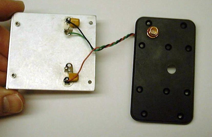
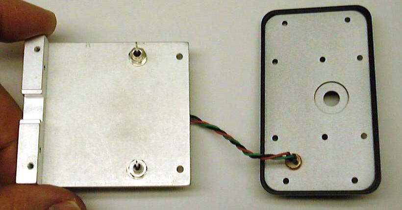
This is the other side of the top aluminum plate showing the power supply pins.
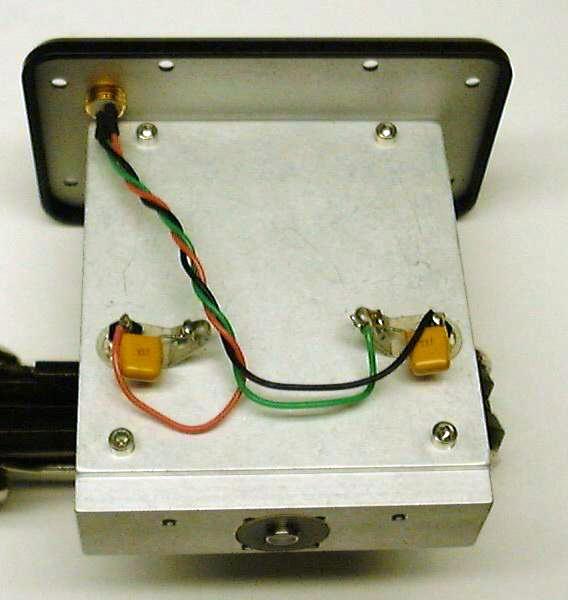
Power supply side when the unit is bolted together. They even twisted the wires to help avoid common-mode noise.
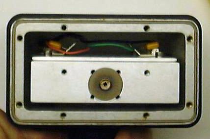
Front fiew of the sensor. You can see the PIN photodiode in the center. Not much room for
stray signals to get in huh?
There is a conductive gasket like an O-ring going all around the front to connect
the front cover electrically to the sides.
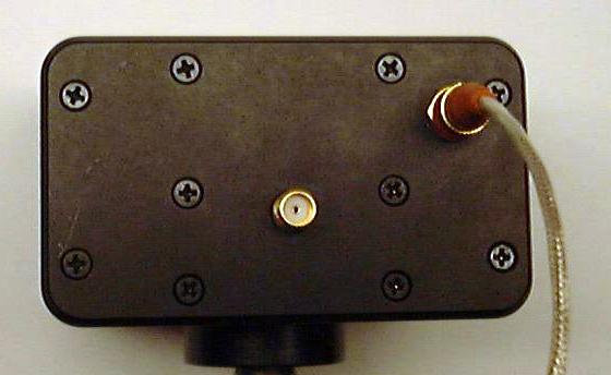
The back of the unit. Shielded power supply connections, and a coax output connector.